And Pcb Design Masterclass 20... | Advanced Hardware
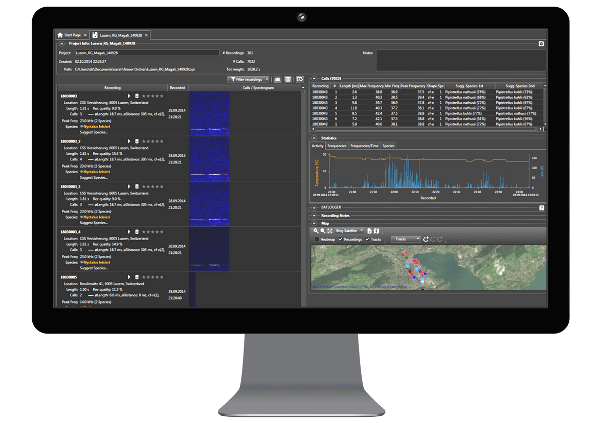
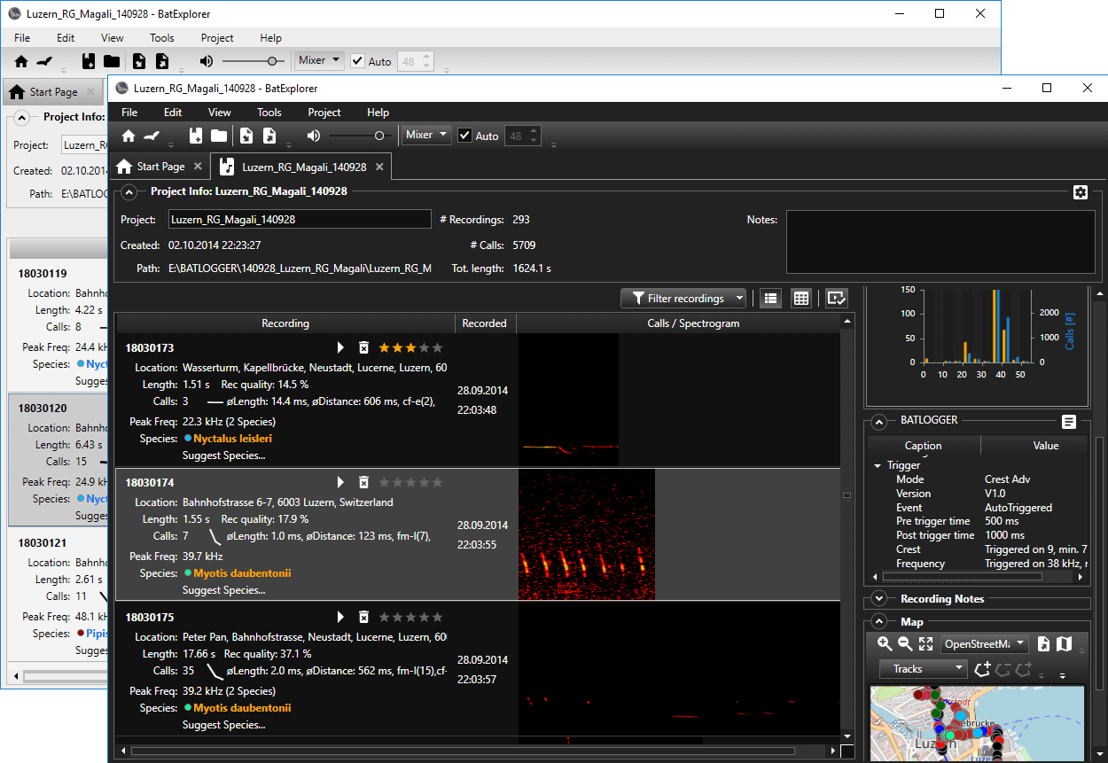
Analyse your recordings
Organize recordings easily and fast
Automatic bat call detection
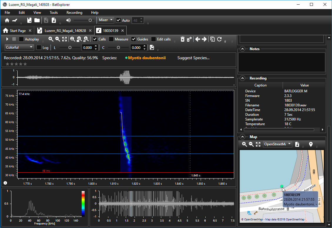
Listening, viewing and classifying recordings
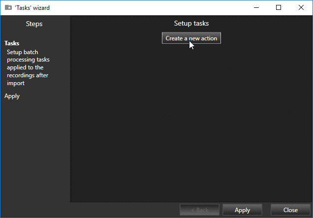
Automate recurring actions with tasks
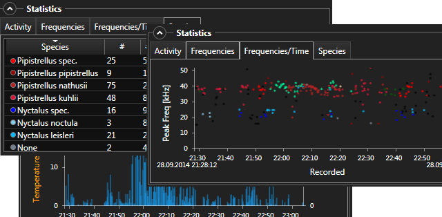
Bat species suggestions
Organize recordings easily and fast
Automatic bat call detection
Listening, viewing and classifying recordings
Automate recurring actions with tasks
Bat species suggestions
Standard FR-4 is inadequate for high-speed designs due to high dielectric loss and dispersion. Engineers must evaluate advanced materials like Rogers, Megtron 6, and Isola laminates. Key metrics include low dissipation factors (
Different materials expand at different rates when heated, defined by their Coefficient of Thermal Expansion (CTE).
This public link is valid for 7 days and shares a thread, including any personal information you added. This link or copies made by others cannot be deleted. If you share with third parties, their policies apply. Can’t copy the link right now. Try again later.
Introduction Modern electronics demand unprecedented speed, efficiency, and miniaturization. Consumer gadgets, automotive systems, and aerospace platforms all push hardware boundaries. Standard design workflows no longer suffice for these tight tolerances. Engineers must evolve past basic routing to master physics-driven layout methodologies. Advanced Hardware and PCB Design Masterclass 20...
What are you routing? (e.g., PCIe Gen 5, DDR5, USB4, RF) What is your target layer count or board size limitation ?
[Top Layer: Signal / Components] <-- 0.5 oz Cu + Plating =================== Prepreg =================== <-- Ultra-low loss (e.g., Megtron 6) [Layer 2: Solid Reference Plane] <-- 1.0 oz Cu (GND) ==================== Core ===================== <-- Thin core for tight coupling [Layer 3: High-Speed Routing] <-- 0.5 oz Cu (Stripline) =================== Prepreg =================== ----------------- CENTER LINE ----------------- <-- Symmetry Axis =================== Prepreg =================== [Layer 4: High-Speed Routing] <-- 0.5 oz Cu (Stripline) ==================== Core ===================== [Layer 5: Solid Reference Plane] <-- 1.0 oz Cu (Power/GND) =================== Prepreg =================== [Bottom Layer: Signal / Components] <-- 0.5 oz Cu + Plating Copper Roughness
This masterclass article delivers advanced strategies for high-speed hardware and printed circuit board (PCB) design. You will explore critical techniques to ensure signal integrity, optimize power delivery, and achieve first-pass manufacturing success. 1. High-Speed Signal Integrity (SI) Standard FR-4 is inadequate for high-speed designs due
An theoretically flawless design is useless if a fabrication house cannot build it reliably or at a reasonable yield. Key DFM Metrics
Use an inner diameter of 0.3mm. Larger holes run the risk of solder wicking right through the board during assembly, starving the component pad. Plating Thickening: Specify
Engineers must deliver faster speeds while reducing power, driving the adoption of advanced packaging techniques. This public link is valid for 7 days
Link internal layers together, completely hidden from the outer surfaces.
As components shrink, power density increases. A 100W processor in a BGA package requires more than just a heatsink; it requires a thermal via strategy .
Signal integrity defines how cleanly a signal travels from driver to receiver. At gigabit speeds, traces behave like transmission lines rather than simple wires. Controlled Impedance
By the final night, the solder smoke clears. You’re not just looking at a piece of fiberglass and copper; you’re looking at a masterpiece of . You’ve learned that in advanced hardware, the smallest trace can be the difference between a breakthrough and a "brick."
Engineers use 2D electromagnetic field solvers to calculate trace geometry based on:
More information about the software can be found in the Online User Guide.